


描述
Waferbonder配置
無配置OEM 代工型號說明
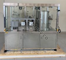
Automated production bonding system for a wide range of fusion/molecular wafer bonding applications SOI wafers are a promising new basic material for the microelectronics industry to produce faster and higher-performance microelectronic devices. Wafer bonding, as one key enabling technology for the SOI wafer fabrication process, achieves high-quality single-crystal silicon films on insulating substrates. With the EVG850 SOI production bonding system, all essential steps for SOI bonding – from cleaning and alignment to pre-bonding and IR-inspection – are combined. Thus, the EVG850 assures a high-yield production process for void-free SOI wafers up to 300 mm sizes. Being the only production system built to operate in high-throughput, high-yield environments, the EVG850 has been established as the industry standard in the SOI wafer market.文檔
無文檔

類別
Wafer Bonders
上次驗證: 超過60天前
關鍵商品詳情
條件:
Used
作業狀態:
未知
產品編號:
41200
晶圓尺寸:
8"/200mm
年份:
2012
Logistics Support
Available
Transaction Insured by Moov
Available
Refurbishment Services
Available
類似上架商品
查看全部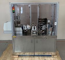


EVGroup (EVG)
EVG850
類別
Wafer Bonders
上次驗證: 超過60天前


關鍵商品詳情
條件:
Used
作業狀態:
未知
產品編號:
41200
晶圓尺寸:
8"/200mm
年份:
2012
Logistics Support
Available
Transaction Insured by Moov
Available
Refurbishment Services
Available
描述
Waferbonder配置
無配置OEM 代工型號說明
Automated production bonding system for a wide range of fusion/molecular wafer bonding applications SOI wafers are a promising new basic material for the microelectronics industry to produce faster and higher-performance microelectronic devices. Wafer bonding, as one key enabling technology for the SOI wafer fabrication process, achieves high-quality single-crystal silicon films on insulating substrates. With the EVG850 SOI production bonding system, all essential steps for SOI bonding – from cleaning and alignment to pre-bonding and IR-inspection – are combined. Thus, the EVG850 assures a high-yield production process for void-free SOI wafers up to 300 mm sizes. Being the only production system built to operate in high-throughput, high-yield environments, the EVG850 has been established as the industry standard in the SOI wafer market.文檔
無文檔