


描述
無描述配置
3 DxZ Chambers w/ RPSOEM 代工型號說明
The Centura 5200 DXZ is used for advanced 150mm and 200mm CVD technology in the advanced CMOS and MtM segments. It can be used for ultra-thick oxides (≥20µm), low-temperature processing (<200°C), conformal, low wet-etch-rate films, and doped films with tunable refractive indices. The system can handle a variety of MtM substrates (including SiC wafers) reliably and carefully from load lock wafer mapping to clear wafer orientation to wafer placement.文檔
無文檔

類別
PECVD
上次驗證: 超過60天前
關鍵商品詳情
條件:
Used
作業狀態:
未知
產品編號:
15128
晶圓尺寸:
8"/200mm
年份:
未知
Logistics Support
Available
Transaction Insured by Moov
Available
Refurbishment Services
Available
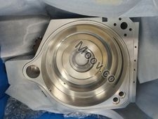

APPLIED MATERIALS (AMAT)
CENTURA 5200 DXZ
類別
PECVD
上次驗證: 超過60天前


關鍵商品詳情
條件:
Used
作業狀態:
未知
產品編號:
15128
晶圓尺寸:
8"/200mm
年份:
未知
Logistics Support
Available
Transaction Insured by Moov
Available
Refurbishment Services
Available
描述
無描述配置
3 DxZ Chambers w/ RPSOEM 代工型號說明
The Centura 5200 DXZ is used for advanced 150mm and 200mm CVD technology in the advanced CMOS and MtM segments. It can be used for ultra-thick oxides (≥20µm), low-temperature processing (<200°C), conformal, low wet-etch-rate films, and doped films with tunable refractive indices. The system can handle a variety of MtM substrates (including SiC wafers) reliably and carefully from load lock wafer mapping to clear wafer orientation to wafer placement.文檔
無文檔