


描述
無描述配置
無配置OEM 代工型號說明
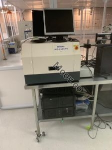
The Semilab WT-2000PVN is a compact measurement system that can perform a range of measurements on photovoltaic (PV) cells, wafers, and blocks. The system comes with overhead functions and can be customized to meet your specific measurement needs by choosing from the available options. The WT-2000PVN is capable of measuring both blocks and ingots, as well as wafers and cells. When measuring wafers and cells, maps are typically produced, while line scans are often used for blocks or ingots to save time. However, the WT-2000PVN can do both. Many PV cell manufacturers use the WT-2000PVN for engineering development, characterization, production batch testing, and troubleshooting production issues. The system can be integrated with various measurement techniques, including µ-PCD/carrier lifetime, SHR/sheet resistance, LBIC/photovoltaic response, quantum efficiency, diffusion length, and eddy current/non-contact resistivity mapping.文檔
無文檔


SEMILAB
WT-2000PV
類別
Defect Inspection
上次驗證: 超過60天前


關鍵商品詳情
條件:
Used
作業狀態:
未知
產品編號:
57413
晶圓尺寸:
未知
年份:
2008
Logistics Support
Available
Transaction Insured by Moov
Available
Refurbishment Services
Available
描述
無描述配置
無配置OEM 代工型號說明
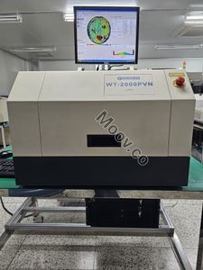
The Semilab WT-2000PVN is a compact measurement system that can perform a range of measurements on photovoltaic (PV) cells, wafers, and blocks. The system comes with overhead functions and can be customized to meet your specific measurement needs by choosing from the available options. The WT-2000PVN is capable of measuring both blocks and ingots, as well as wafers and cells. When measuring wafers and cells, maps are typically produced, while line scans are often used for blocks or ingots to save time. However, the WT-2000PVN can do both. Many PV cell manufacturers use the WT-2000PVN for engineering development, characterization, production batch testing, and troubleshooting production issues. The system can be integrated with various measurement techniques, including µ-PCD/carrier lifetime, SHR/sheet resistance, LBIC/photovoltaic response, quantum efficiency, diffusion length, and eddy current/non-contact resistivity mapping.文檔
無文檔