


描述
無描述配置
無配置OEM 代工型號說明
The AIT III is a high-throughput darkfield wafer inspection tool that can capture small defects resulting from the transition to 0.13 µm and smaller design rules. It has advanced noise suppression capabilities, making it suitable for films, CMP, photo, and etch applications. It is ideal for the development and ramp of 0.13 µm technology products and extends a fab’s current capability for production tool monitoring of yield-limiting defects. It offers improved capture of CMP and pattern transfer defects, superior suppression of grain, pattern noise and color variation, high defect signal-to-noise ratio with maximized surface selectivity, high throughput at required sensitivity, fast automated recipe setup, rigorous system-to-system matching, and is field upgradeable from the AIT II. It is also 300 mm capable with flexible automation options.文檔
無文檔

類似上架商品
查看全部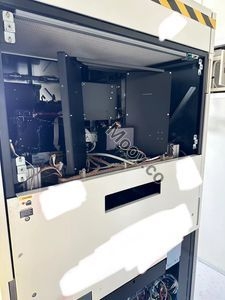


KLA
AIT III
類別
Defect Inspection
上次驗證: 超過60天前


關鍵商品詳情
條件:
Used
作業狀態:
未知
產品編號:
102930
晶圓尺寸:
未知
年份:
未知
Logistics Support
Available
Transaction Insured by Moov
Available
Refurbishment Services
Available
描述
無描述配置
無配置OEM 代工型號說明
The AIT III is a high-throughput darkfield wafer inspection tool that can capture small defects resulting from the transition to 0.13 µm and smaller design rules. It has advanced noise suppression capabilities, making it suitable for films, CMP, photo, and etch applications. It is ideal for the development and ramp of 0.13 µm technology products and extends a fab’s current capability for production tool monitoring of yield-limiting defects. It offers improved capture of CMP and pattern transfer defects, superior suppression of grain, pattern noise and color variation, high defect signal-to-noise ratio with maximized surface selectivity, high throughput at required sensitivity, fast automated recipe setup, rigorous system-to-system matching, and is field upgradeable from the AIT II. It is also 300 mm capable with flexible automation options.文檔
無文檔