We value your privacy
We and our selected partners use cookies to enhance your browsing experience, serve personalized content, and analyze our traffic. By clicking "Accept All", you consent to our use of cookies. 閱讀詳情


無文檔
上次驗證: 超過60天前
Refurbished
未知
85052
未知
未知
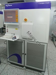
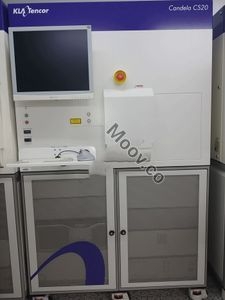
KLA
Refurbished
未知
85052
未知
未知
無文檔