


描述
Wafer CV mapper - Mercury Probe 1.2 System Specifications 1. Wafer size: 1-inch to 12-inch wafers typical (8-inch for 92A/92B), sample size can be as small as 5mm x 5mm 2. Polar or Cartesian mapping up to 49 sites with edge exclusion up to 1.5 mm 3. MOS Doping Profiles: Dope: 8 x 10¹² to 5 x 10¹⁸ ions/cm3 Depth: 0 to 10 Microns. Repeatability: ±1.5% typical 4. Interface Trap Density (DIT) Range: 2 x 10¹⁰ states/cm2 to 2 x 10¹² states/cm2 Repeatability: ±5% or ±1010 states/ cm2 whichever is larger 5. Oxide Thickness Range: 24A to 20,000A by C-V method, 15A to 30A by I-V method 6. Ion Implant Dose Range: 1 x 10¹¹ to 5 x 10¹² ions/cm2 Repeatability: ±1% typical 7. Epitaxial Doping Density Range: 1 x 10¹⁴ to 1 x 1018 cm-3 Repeatability: ±2% typical 8. Epitaxial Thickness Range: 0.3 to 3 microns Repeatability: ±3% typical 9. Generation Lifetime Range: 0.01us to 100ms Repeatability: ±10% typical 10. Insulating Film and Semi-Insulating Layer Resistivity Range: 1 x 10⁶ to 1 x 10¹⁶ Ohm-cm in 30A to 1 mm thickness 11. Current range: 50 fA to 1 mA 12. Bias voltage: -100 to 100 Volts 13. Measurement pulse: 50mV, 100 mV, or 150 mV, > 20us for Ch, >lms for Cq 14. Probe: mercury dot only, mercury dot and one mercury ring, mercury dot with two mercury ring or external 15. Compressed Air: 60Psi at 1.5 liter per minute maximum flow 16. Vacuum: 28-inch Hg minimum at 0.5 liter/min maximum flow 1.3 Operation Features The system software consists of six main parts: (1) The basic software has programs for measuring quasi-static, high frequency and deep pulsed C-V, displaying the curves, generating maps and storing data. (2) The program that uses C-V curves to determine doping profile and dosage of low dose implantation, epi and raw wafer. (3) The program that determines gate Oxide TDDB and Qbd, obtains Oxide I-V curves, checks the trap densities, and maps Oxide thickness. (4) The generation lifetime program that obtains carrier generation lifetime at different depth through measuring generation current at different biases. (5) The program for GaAs which maps dosage of epi and ion implantation; it also maps semi-insulating layer resistivities. (6) The program using psuedo MOST technique to characterize SOI. 1.4 System Composition The system hardware mainly consists of: (1) The CVmap 92A/92B mercury instrument and its attachments that include hoses for vacuum, compressed air and N2 (2) The system computer, a monitor, a printer, and a RS-232 cable for the communication between the CVmap instrument and the system computer. (3) Mercury Spill Control Station (4) Optional needle probe station for probing at pads.配置
Mercury Probe for Substrates from 5mm X 5mm to 200mm Wafers • Dose Monitoring for Silicon and GaAs Wafers • Wafer Mapping up to 49 Test Points • System Control Computer 4D Application SW Version 1.28 • Windows 2000 Professional OS, CD-ROM, FDD, Flat Screen Monitor, Keyboard & Mouse • Embedded Computer FDD Flat Screen Monitor, Keyboard • 115V, 1Ph., 60 Hz, 16AOEM 代工型號說明
Probers文檔
無文檔

類別
Resistivity / Four Point Probe
上次驗證: 24 天前
關鍵商品詳情
條件:
Used
作業狀態:
未知
產品編號:
148417
晶圓尺寸:
8"/200mm
年份:
2005
Logistics Support
Available
Transaction Insured by Moov
Available
Refurbishment Services
Available
類似上架商品
查看全部


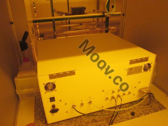
FOUR DIMENSIONS
CVMap3092A
類別
Resistivity / Four Point Probe
上次驗證: 24 天前


關鍵商品詳情
條件:
Used
作業狀態:
未知
產品編號:
148417
晶圓尺寸:
8"/200mm
年份:
2005
Logistics Support
Available
Transaction Insured by Moov
Available
Refurbishment Services
Available
描述
Wafer CV mapper - Mercury Probe 1.2 System Specifications 1. Wafer size: 1-inch to 12-inch wafers typical (8-inch for 92A/92B), sample size can be as small as 5mm x 5mm 2. Polar or Cartesian mapping up to 49 sites with edge exclusion up to 1.5 mm 3. MOS Doping Profiles: Dope: 8 x 10¹² to 5 x 10¹⁸ ions/cm3 Depth: 0 to 10 Microns. Repeatability: ±1.5% typical 4. Interface Trap Density (DIT) Range: 2 x 10¹⁰ states/cm2 to 2 x 10¹² states/cm2 Repeatability: ±5% or ±1010 states/ cm2 whichever is larger 5. Oxide Thickness Range: 24A to 20,000A by C-V method, 15A to 30A by I-V method 6. Ion Implant Dose Range: 1 x 10¹¹ to 5 x 10¹² ions/cm2 Repeatability: ±1% typical 7. Epitaxial Doping Density Range: 1 x 10¹⁴ to 1 x 1018 cm-3 Repeatability: ±2% typical 8. Epitaxial Thickness Range: 0.3 to 3 microns Repeatability: ±3% typical 9. Generation Lifetime Range: 0.01us to 100ms Repeatability: ±10% typical 10. Insulating Film and Semi-Insulating Layer Resistivity Range: 1 x 10⁶ to 1 x 10¹⁶ Ohm-cm in 30A to 1 mm thickness 11. Current range: 50 fA to 1 mA 12. Bias voltage: -100 to 100 Volts 13. Measurement pulse: 50mV, 100 mV, or 150 mV, > 20us for Ch, >lms for Cq 14. Probe: mercury dot only, mercury dot and one mercury ring, mercury dot with two mercury ring or external 15. Compressed Air: 60Psi at 1.5 liter per minute maximum flow 16. Vacuum: 28-inch Hg minimum at 0.5 liter/min maximum flow 1.3 Operation Features The system software consists of six main parts: (1) The basic software has programs for measuring quasi-static, high frequency and deep pulsed C-V, displaying the curves, generating maps and storing data. (2) The program that uses C-V curves to determine doping profile and dosage of low dose implantation, epi and raw wafer. (3) The program that determines gate Oxide TDDB and Qbd, obtains Oxide I-V curves, checks the trap densities, and maps Oxide thickness. (4) The generation lifetime program that obtains carrier generation lifetime at different depth through measuring generation current at different biases. (5) The program for GaAs which maps dosage of epi and ion implantation; it also maps semi-insulating layer resistivities. (6) The program using psuedo MOST technique to characterize SOI. 1.4 System Composition The system hardware mainly consists of: (1) The CVmap 92A/92B mercury instrument and its attachments that include hoses for vacuum, compressed air and N2 (2) The system computer, a monitor, a printer, and a RS-232 cable for the communication between the CVmap instrument and the system computer. (3) Mercury Spill Control Station (4) Optional needle probe station for probing at pads.配置
Mercury Probe for Substrates from 5mm X 5mm to 200mm Wafers • Dose Monitoring for Silicon and GaAs Wafers • Wafer Mapping up to 49 Test Points • System Control Computer 4D Application SW Version 1.28 • Windows 2000 Professional OS, CD-ROM, FDD, Flat Screen Monitor, Keyboard & Mouse • Embedded Computer FDD Flat Screen Monitor, Keyboard • 115V, 1Ph., 60 Hz, 16AOEM 代工型號說明
Probers文檔
無文檔