


描述
無描述配置
無配置OEM 代工型號說明
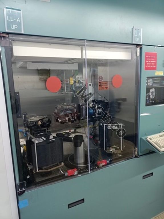
The Eclipse Mark IV is the latest generation PVD tool from the highly successful Eclipse family. It offers the lowest Cost-of-Ownership through high throughput, a small footprint, and high reliability with exceptional process performance. The system achieves high throughput in a high vacuum environment through the use of serial wafer handling, resulting in 80% fewer wafer transfers than a traditional cluster tool. The Eclipse Mark IV has a footprint of 44 square feet and can be configured for etch or deposition, providing full capability for today’s contact, barrier, interconnect, resistor, and packaging films for Silicon, GaAs and CCD substrates. Wafer temperature is regulated by backplane heaters and the chambers have world class vacuum leak rates and base pressures.文檔
無文檔

類別
PVD / Sputtering
上次驗證: 超過60天前
關鍵商品詳情
條件:
Used
作業狀態:
Installed / Idle
產品編號:
135783
晶圓尺寸:
8"/200mm
年份:
1999
Logistics Support
Available
Transaction Insured by Moov
Available
Refurbishment Services
Available


TEL / MRC
ECLIPSE MARK IV
類別
PVD / Sputtering
上次驗證: 超過60天前


關鍵商品詳情
條件:
Used
作業狀態:
Installed / Idle
產品編號:
135783
晶圓尺寸:
8"/200mm
年份:
1999
Logistics Support
Available
Transaction Insured by Moov
Available
Refurbishment Services
Available
描述
無描述配置
無配置OEM 代工型號說明
The Eclipse Mark IV is the latest generation PVD tool from the highly successful Eclipse family. It offers the lowest Cost-of-Ownership through high throughput, a small footprint, and high reliability with exceptional process performance. The system achieves high throughput in a high vacuum environment through the use of serial wafer handling, resulting in 80% fewer wafer transfers than a traditional cluster tool. The Eclipse Mark IV has a footprint of 44 square feet and can be configured for etch or deposition, providing full capability for today’s contact, barrier, interconnect, resistor, and packaging films for Silicon, GaAs and CCD substrates. Wafer temperature is regulated by backplane heaters and the chambers have world class vacuum leak rates and base pressures.文檔
無文檔