


描述
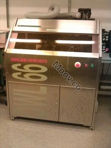
The Heidelberg Instruments DWL-66 is a versatile laser-based system designed for advanced mask production and wafer patterning. Utilizing a HeCd laser, it achieves fine resolution down to 800 nm through meticulous alignment and control of the laser optics. Fully operational and still installed.配置
442 nm wavelength, 300 mW, HeCd laser (replaced in 2014, has around 4400 hours of usage) 4 mm write head 20 mm write head Flowbox Greyscale exposure Upgraded computer to Windows 7 in 2019 Metrology and Alignment PackageOEM 代工型號說明
The DWL 66 is a precise, maskless laser lithography system for various applications like maskless lithography, photomask making, and direct writing. It supports gray-scale exposures on flat, photosensitive-coated materials. Key features include a minimum feature size of 0.6 microns, substrate size up to 200 x 200 mm, and over 1.0M dpi resolution using a 20-nanometer address grid.文檔
無文檔

類別
Lithography
上次驗證: 超過60天前
關鍵商品詳情
條件:
Used
作業狀態:
Installed / Running
產品編號:
115928
晶圓尺寸:
未知
Laser:
442
年份:
2002
Logistics Support
Available
Transaction Insured by Moov
Available
Refurbishment Services
Available

HEIDELBERG INSTRUMENTS
DWL 66
類別
Lithography
上次驗證: 超過60天前


關鍵商品詳情
條件:
Used
作業狀態:
Installed / Running
產品編號:
115928
晶圓尺寸:
未知
Laser:
442
年份:
2002
Logistics Support
Available
Transaction Insured by Moov
Available
Refurbishment Services
Available
描述
The Heidelberg Instruments DWL-66 is a versatile laser-based system designed for advanced mask production and wafer patterning. Utilizing a HeCd laser, it achieves fine resolution down to 800 nm through meticulous alignment and control of the laser optics. Fully operational and still installed.配置
442 nm wavelength, 300 mW, HeCd laser (replaced in 2014, has around 4400 hours of usage) 4 mm write head 20 mm write head Flowbox Greyscale exposure Upgraded computer to Windows 7 in 2019 Metrology and Alignment PackageOEM 代工型號說明
The DWL 66 is a precise, maskless laser lithography system for various applications like maskless lithography, photomask making, and direct writing. It supports gray-scale exposures on flat, photosensitive-coated materials. Key features include a minimum feature size of 0.6 microns, substrate size up to 200 x 200 mm, and over 1.0M dpi resolution using a 20-nanometer address grid.文檔
無文檔