


描述
SSM 530 HG-CV System for EPI resistivity配置
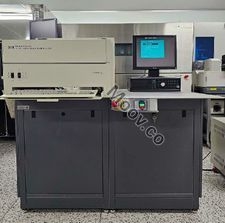
Capable up to 12" Wafer with manual wafer loading: 6" setting SSM 52 Capacitance Measurement Unit Motor control unit Pneumatic control Unit PC System PROCAP software : H5100 V6.42 Performance - CV Meter Noise Test (Schottky Diode Test): 1 STD(%) <0.167% - MOS Wafer Test : 1 STD(%) <0.167% Others : -MOS reference wafer -Packaged Schottkey Diode -Hg Spill station ■ Capacitance: 0.5~ 2000pF ■ Conductance: 0.5 ~ 2000μS ■ DC Bias voltage: ± 250V ■ Ramp Rate: 0 ~ 50 V/s continuously variable ■ Drive Signal Frequency at 1Mhz voltage=15mV rms ■Stress Voltage: ± 250V ■ CDA: 80~100psi, Nitrogen for sample purge:0~15psi ■ Ambient temperature: 18° - 25°C ± 2°C over 24 hour periodOEM 代工型號說明
The SSM 530 is a fully automatic mapping system that provides a variety of electrical characterization measurements for non-patterned wafers used in epitaxial silicon production and front-end semiconductor processing. It has the same abilities as the SSM 5130, but it does not have a robot. The SSM 530 eliminates the need for costly metal and poly deposition processes by using a pneumatically controlled, non-damaging probe design and a top-side mercury contact. It features an extremely stable contact area and uses only a small quantity of mercury to make highly repeatable measurements for process development and process monitoring applications. Typical applications include EPI resistivity, low-k dielectric constant, and oxide integrity. The system can handle wafer diameters from 200 mm to 300 mm and can perform single-site and multiple-site maps. It also features automatic face-up loading to prevent wafer damage, precision pressure regulators for Hg contact, and PROCAP software that provides a full suite of measurements.文檔
無文檔


SSM
530
類別
EPI Resistivity Measurement
上次驗證: 超過60天前


關鍵商品詳情
條件:
Refurbished
作業狀態:
未知
產品編號:
66045
晶圓尺寸:
12"/300mm
年份:
2008
Logistics Support
Available
Transaction Insured by Moov
Available
Refurbishment Services
Available
描述
SSM 530 HG-CV System for EPI resistivity配置
Capable up to 12" Wafer with manual wafer loading: 6" setting SSM 52 Capacitance Measurement Unit Motor control unit Pneumatic control Unit PC System PROCAP software : H5100 V6.42 Performance - CV Meter Noise Test (Schottky Diode Test): 1 STD(%) <0.167% - MOS Wafer Test : 1 STD(%) <0.167% Others : -MOS reference wafer -Packaged Schottkey Diode -Hg Spill station ■ Capacitance: 0.5~ 2000pF ■ Conductance: 0.5 ~ 2000μS ■ DC Bias voltage: ± 250V ■ Ramp Rate: 0 ~ 50 V/s continuously variable ■ Drive Signal Frequency at 1Mhz voltage=15mV rms ■Stress Voltage: ± 250V ■ CDA: 80~100psi, Nitrogen for sample purge:0~15psi ■ Ambient temperature: 18° - 25°C ± 2°C over 24 hour periodOEM 代工型號說明
The SSM 530 is a fully automatic mapping system that provides a variety of electrical characterization measurements for non-patterned wafers used in epitaxial silicon production and front-end semiconductor processing. It has the same abilities as the SSM 5130, but it does not have a robot. The SSM 530 eliminates the need for costly metal and poly deposition processes by using a pneumatically controlled, non-damaging probe design and a top-side mercury contact. It features an extremely stable contact area and uses only a small quantity of mercury to make highly repeatable measurements for process development and process monitoring applications. Typical applications include EPI resistivity, low-k dielectric constant, and oxide integrity. The system can handle wafer diameters from 200 mm to 300 mm and can perform single-site and multiple-site maps. It also features automatic face-up loading to prevent wafer damage, precision pressure regulators for Hg contact, and PROCAP software that provides a full suite of measurements.文檔
無文檔