


描述
無描述配置
無配置OEM 代工型號說明
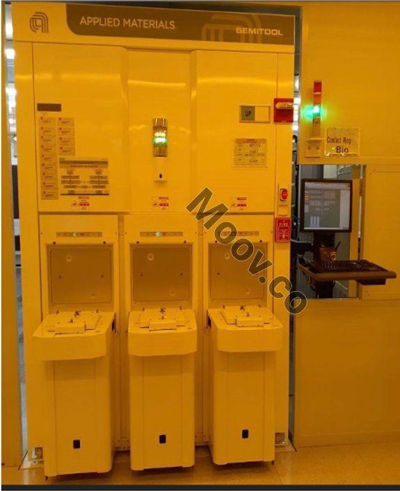
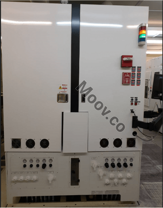
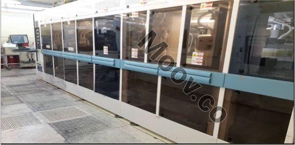
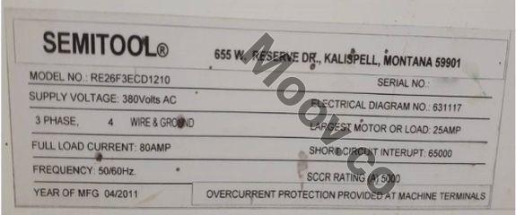
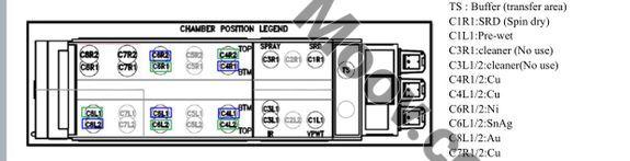
The Raider-S ECD is a high-volume single-wafer electroplating tool designed for Through-Silicon Via (TSV) and Wafer Level Packaging (WLP) applications. It features a precision, fully automated wafer handling system coupled with individual process chambers and is compatible with automated chemical management systems. The Raider-S ECD offers advanced metal deposition or clean chambers, with the option of 15 to over 27 process chambers. It also incorporates chemical analysis options, membrane plating technology, and a multi-zone anode for thinned seed plating. The Raider-S ECD has a small footprint and is available in 200mm or 300mm wafer sizes. Its applications include electrolytic metal deposition, such as Cu-TSV, Pillar, and SnAg bumping. With its advanced features and capabilities, the Raider-S ECD is a powerful tool for advanced semiconductor manufacturing.文檔
無文檔

類別
Electro Plating
上次驗證: 超過60天前
關鍵商品詳情
條件:
Used
作業狀態:
未知
產品編號:
40625
晶圓尺寸:
未知
年份:
2011
Logistics Support
Available
Transaction Insured by Moov
Available
Refurbishment Services
Available
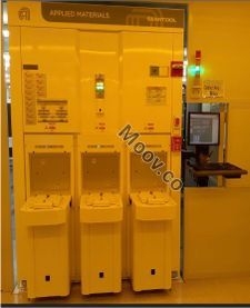

APPLIED MATERIALS (AMAT) / SEMITOOL
RAIDER S ECD
類別
Electro Plating
上次驗證: 超過60天前

關鍵商品詳情
條件:
Used
作業狀態:
未知
產品編號:
40625
晶圓尺寸:
未知
年份:
2011
Logistics Support
Available
Transaction Insured by Moov
Available
Refurbishment Services
Available
描述
無描述配置
無配置OEM 代工型號說明
The Raider-S ECD is a high-volume single-wafer electroplating tool designed for Through-Silicon Via (TSV) and Wafer Level Packaging (WLP) applications. It features a precision, fully automated wafer handling system coupled with individual process chambers and is compatible with automated chemical management systems. The Raider-S ECD offers advanced metal deposition or clean chambers, with the option of 15 to over 27 process chambers. It also incorporates chemical analysis options, membrane plating technology, and a multi-zone anode for thinned seed plating. The Raider-S ECD has a small footprint and is available in 200mm or 300mm wafer sizes. Its applications include electrolytic metal deposition, such as Cu-TSV, Pillar, and SnAg bumping. With its advanced features and capabilities, the Raider-S ECD is a powerful tool for advanced semiconductor manufacturing.文檔
無文檔