


描述
無描述配置
無配置OEM 代工型號說明
AutoWafer is an ultrasonic wafer scanner for nondestructive testing (NDT) of wafers in development and production environments, providing high-resolution identification of bond defects in wafer applications such as MEMS, CMOS, memory, TSV and LED. Robotic cassette handling and sorting of approved and failed wafers helps speed production, while our advanced transducers and auto-analysis tools make it quick and easy to identify even the smallest, most subtle defects. -The ideal automatic ultrasonic testing system for detecting wafer-to-wafer bonding defects -A fully automated, production-ready wafer scanner for MEMS, CMOS, BSI sensors, memory, TSV, LED and other applications employing wafers 200mm and smaller -Provides wafer map with die-level pass/fail indicators (optional) -Provides analysis (optional) -200mm SECS/GEM -TSV entrenched metrology文檔
無文檔

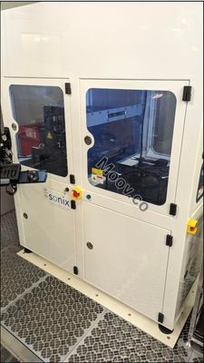
SONIX
AutoWafer
類別
Defect Inspection
上次驗證: 超過60天前


關鍵商品詳情
條件:
Used
作業狀態:
未知
產品編號:
72971
晶圓尺寸:
未知
年份:
未知
Logistics Support
Available
Transaction Insured by Moov
Available
Refurbishment Services
Available
描述
無描述配置
無配置OEM 代工型號說明
AutoWafer is an ultrasonic wafer scanner for nondestructive testing (NDT) of wafers in development and production environments, providing high-resolution identification of bond defects in wafer applications such as MEMS, CMOS, memory, TSV and LED. Robotic cassette handling and sorting of approved and failed wafers helps speed production, while our advanced transducers and auto-analysis tools make it quick and easy to identify even the smallest, most subtle defects. -The ideal automatic ultrasonic testing system for detecting wafer-to-wafer bonding defects -A fully automated, production-ready wafer scanner for MEMS, CMOS, BSI sensors, memory, TSV, LED and other applications employing wafers 200mm and smaller -Provides wafer map with die-level pass/fail indicators (optional) -Provides analysis (optional) -200mm SECS/GEM -TSV entrenched metrology文檔
無文檔