


描述
無描述配置
無配置OEM 代工型號說明
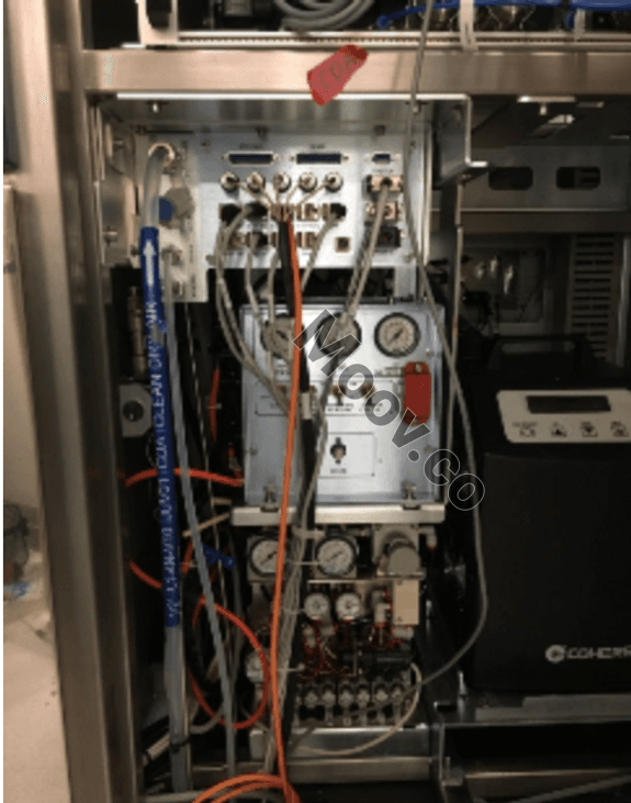
Applied UVision® 3 system, the industry’s highest productivity DUV1 Brightfield wafer inspection tool with the critical-defect detection sensitivity required for 45 nanometer (nm) FEOL2 and immersion lithography. Delivering significant advancements to Applied’s breakthrough UVision technology, this next-generation system triples the number of laser beams scanning the wafer to provide 40% faster throughput than any competitive system. Two new imaging modes extend sensitivity to 20nm, and a new flexible automatic defect classification engine enables quick access to defects of interest and faster yield learning. imaging modes in the illumination and collection path which address the contrast versatility required for periphery areas; innovative algorithms of high defect accuracy and stitch-to-stitch detection enable enhanced sensitivity on edge of array and on high-end devices; dual screen configuration with High Resolution Review, which minimizes SEM review time; and new automatic classification capabilities provide quick access to defect-of-interest to reduce yield learning cycle. Additionally, UVision 3’s proprietary ActiveScan technique dynamically compensates for process and color variations within and across wafers.文檔
無文檔

類別
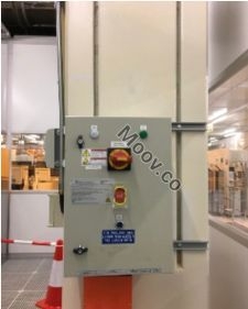
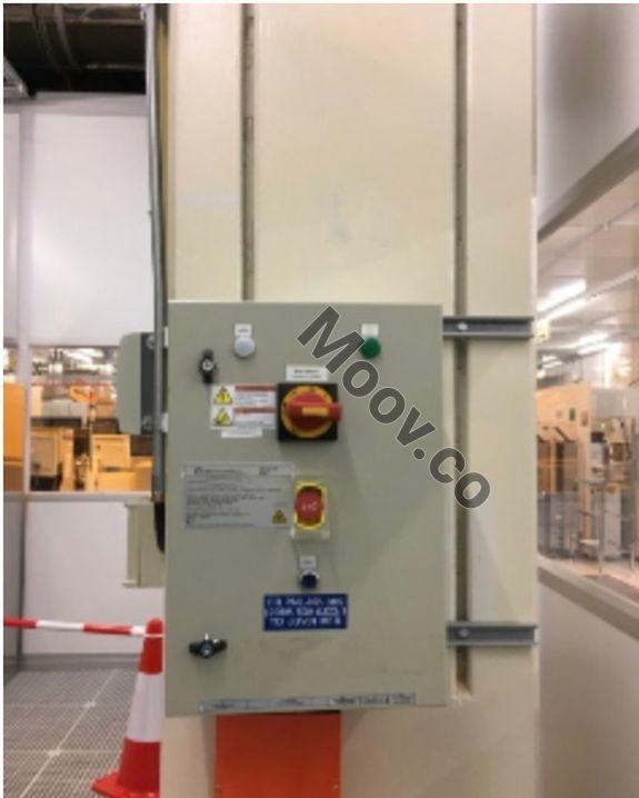
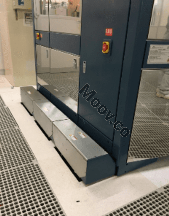
Defect Inspection
上次驗證: 超過60天前
關鍵商品詳情
條件:
Used
作業狀態:
未知
產品編號:
29600
晶圓尺寸:
未知
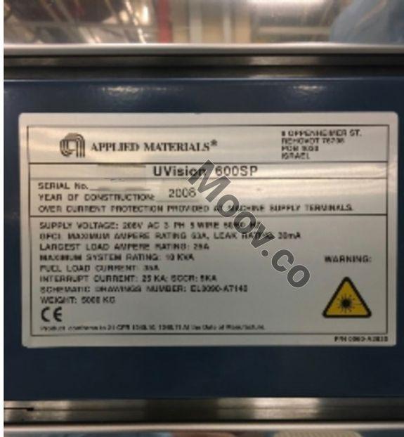
年份:
2008
Logistics Support
Available
Transaction Insured by Moov
Available
Refurbishment Services
Available
APPLIED MATERIALS (AMAT)
UVISION 3
類別
Defect Inspection
上次驗證: 超過60天前

關鍵商品詳情
條件:
Used
作業狀態:
未知
產品編號:
29600
晶圓尺寸:
未知
年份:
2008
Logistics Support
Available
Transaction Insured by Moov
Available
Refurbishment Services
Available
描述
無描述配置
無配置OEM 代工型號說明
Applied UVision® 3 system, the industry’s highest productivity DUV1 Brightfield wafer inspection tool with the critical-defect detection sensitivity required for 45 nanometer (nm) FEOL2 and immersion lithography. Delivering significant advancements to Applied’s breakthrough UVision technology, this next-generation system triples the number of laser beams scanning the wafer to provide 40% faster throughput than any competitive system. Two new imaging modes extend sensitivity to 20nm, and a new flexible automatic defect classification engine enables quick access to defects of interest and faster yield learning. imaging modes in the illumination and collection path which address the contrast versatility required for periphery areas; innovative algorithms of high defect accuracy and stitch-to-stitch detection enable enhanced sensitivity on edge of array and on high-end devices; dual screen configuration with High Resolution Review, which minimizes SEM review time; and new automatic classification capabilities provide quick access to defect-of-interest to reduce yield learning cycle. Additionally, UVision 3’s proprietary ActiveScan technique dynamically compensates for process and color variations within and across wafers.文檔
無文檔