


描述
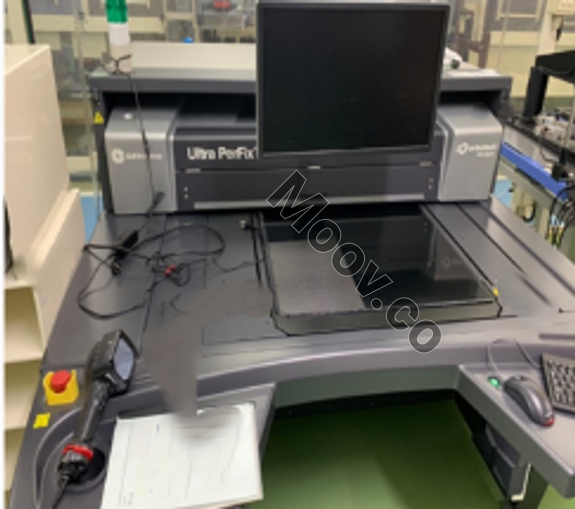
Rework target: L/S 10um or above. Maximum copper foil thickness <70um. PCB MAX 660×610mm. Laser type: YAG LASER, wavelength 532nm, high-energy shape, near-vertical irradiation, processing spot diameter 3µm. Function Description: Uses laser irradiation to eliminate short circuits and copper residue on advanced HDI and IC substrates, including CSP, FC-CSP, BGA and FC-BGA applications. Even for high-density substrate circuit designs, Ultra PerFix 120 can complete precise rework within 1 minute. When analysis reaches 10µm, scrap can be minimized.配置
無配置OEM 代工型號說明
Ultra PerFix 120 automatically shapes excess copper defects down to 10μm resolution. The system delivers breakthrough capabilities for eliminating scrap by achieving perfect results in less than a minute on complex CSP, FC-CSP, BGA and FC-BGA designs.文檔
無文檔

類別
AOI
上次驗證: 超過60天前
關鍵商品詳情
條件:
Used
作業狀態:
未知
產品編號:
58895
晶圓尺寸:
未知
年份:
2013
Logistics Support
Available
Transaction Insured by Moov
Available
Refurbishment Services
Available


KLA / ORBOTECH
ULTRA PERFIX 120
類別
AOI
上次驗證: 超過60天前


關鍵商品詳情
條件:
Used
作業狀態:
未知
產品編號:
58895
晶圓尺寸:
未知
年份:
2013
Logistics Support
Available
Transaction Insured by Moov
Available
Refurbishment Services
Available
描述
Rework target: L/S 10um or above. Maximum copper foil thickness <70um. PCB MAX 660×610mm. Laser type: YAG LASER, wavelength 532nm, high-energy shape, near-vertical irradiation, processing spot diameter 3µm. Function Description: Uses laser irradiation to eliminate short circuits and copper residue on advanced HDI and IC substrates, including CSP, FC-CSP, BGA and FC-BGA applications. Even for high-density substrate circuit designs, Ultra PerFix 120 can complete precise rework within 1 minute. When analysis reaches 10µm, scrap can be minimized.配置
無配置OEM 代工型號說明
Ultra PerFix 120 automatically shapes excess copper defects down to 10μm resolution. The system delivers breakthrough capabilities for eliminating scrap by achieving perfect results in less than a minute on complex CSP, FC-CSP, BGA and FC-BGA designs.文檔
無文檔