EVG620
概述
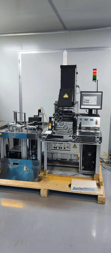
The EVG620 is a versatile tool developed by EV Group (EVG) that serves as both an optical double-side lithography and precision alignment system, specifically designed for wafers up to 100 mm in size. The system is capable of safely handling thick, bowed, or small diameter wafers, providing enhanced flexibility in wafer processing. The EVG620's alignment stage design is a standout feature, delivering highly accurate alignment and exposure results for precise patterning. It is equipped with high-resolution top and bottom side split-field microscopes, ensuring excellent imaging capabilities. The user-friendly interface, based on Windows, streamlines the operation of the EVG620, making it a reliable and efficient tool for various lithography and alignment applications in semiconductor and microelectronics manufacturing.
活躍中的上架商品
25
服務
檢驗、保險、評估、物流